
Password Protection System
In this project the goal was to design a RAM based password protection system using Verilog HDL targeting a FPGA. The major components in developing this system were to design a well functional keypad scanner to receive input, and a RAM system to store and compare the input password to the stored password. In place of an actual lock, the output is displayed on a LED display.
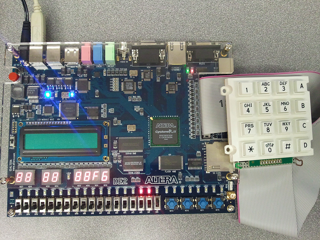
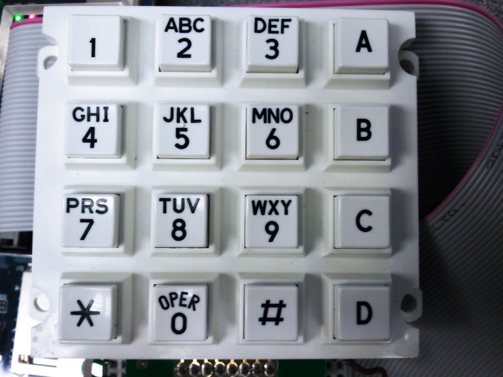
The target board was a DE2 Altera Cyclone II FPGA development board running at 50 MHz. Attached to the I/O port a 16-key keypad was attached providing direct access to the keypad matrix. In operation of the system, the user types the password into the keypad, verifying each key as it is typed on a seven segment display. When password is entered, the user presses the star key, which will light up a LED if the password is correct to indicate the system is unlocked.
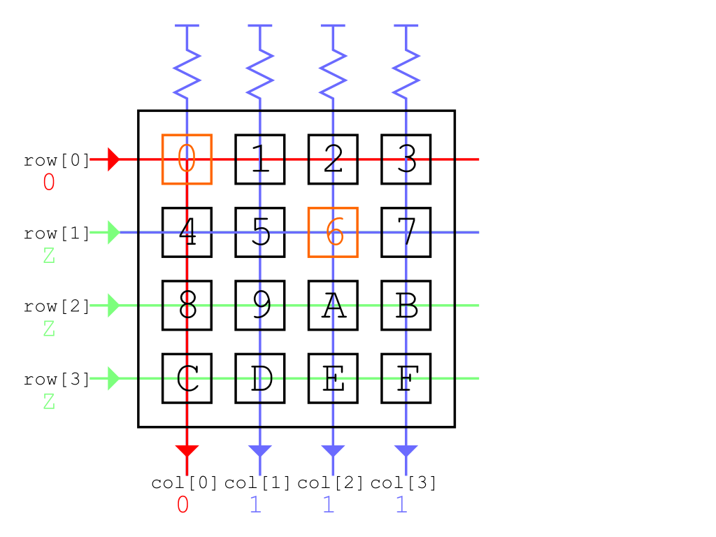
The process of receiving input involves checking the keypad constantly to see if a key is currently being pressed. The keypad matrix internally is a grid of rows and columns, where a key press momentarily connects the row and column under the key. We scanned each row at a time, and checked the value at each column as input to determine the key pressed. By scanning the keypad in this manner, each key can be identified individually regardless of how many are currently pressed, so ghosting is avoided. Still, the mechanical contacts of the key will cause jitter and needed to be debounced. And a basis for timing was necessary to scan at a consistent interval.
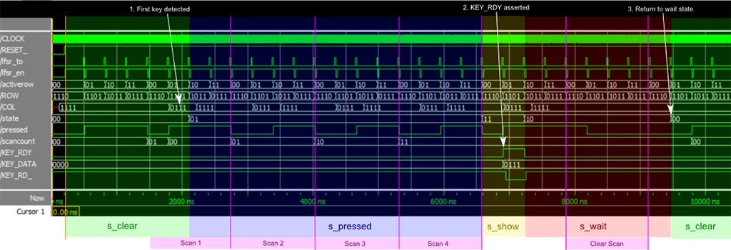
To identify a valid keypress, no keys must be pressed for a single scan of all rows, followed by a single key being pressed for 4 consecutive scans. We targeted a response time of 8ms, in which the four scans must take place. The FPGA however is running at 50 MHz, giving us a period of 20ns, much too fast for this scanning application. To divide the frequency down to be usable for scanning, we utilized a LFSR counter. This counter uses a series of shift registers with XOR feedback to generate a pseudo-random counter in which every output number only occurs once in the sequence. We calculated the number of states necessary and the corresponding counter value to match the desired timing for each row scan. The counter is incremented each cycle until the value is reached, which advances the scanner to the next row.
Once we had developed the LFSR counter, we designed a RTL state machine to perform the key press validation. Many input situations had to be considered for the design of the scanner. If one key is pressed for the desired response time, then it should be recognized. However, if two keys are pressed simultaneously and held, and then one is released, should it be recognized? If a single key is held and recognized, and then an additional key is then pressed, should the second key be recognized? Our testbench used in simulation incorporated many of these situations to verify that the behavior was correct.
Using the previous modules, we added support for the RAM on the development board to store the valid key presses as they are entered. Using another state machine, each recognized key is compared to the password stored within the ROM. If a key does not match the corresponding digit in the password as it is pressed, the system will immediately switch into an invalid state, and will not unlock when the star key is pressed. Alternatively, if all password digits have matched, the system will remain in a valid state and unlock when the star key is pressed. This design also supports mismatched password length detection. In all test cases, the password protection functioned properly without error.